


Return on Investment:
Master semiconductor devices and technologies, from basic concepts to advanced applications in EVs, AI, space, and more. Gain the skills to lead and innovate in this rapidly evolving industry.

Admissions Closed.
Course Duration :
6 months ((75 hours)
Course Fees :
₹ 1,25,000 + 18% GST
Schedule :
Sundays, 9:30 AM – 12:30 PM
Course Eligibility :
B.Tech/M.Sc./10+2+3 diploma holders
Campus Immersion (Optional):
An optional two-day in-person session at IIT Delhi toward the end of the program
Master semiconductor devices and technologies, from basic concepts to advanced applications in EVs, AI, space, and more. Gain the skills to lead and innovate in this rapidly evolving industry.

Learn to design and fabricate cutting-edge semiconductor devices. Position yourself as an expert in emerging technologies like AI and automotive.

Stay ahead of the semiconductor revolution by understanding market trends and commercial opportunities. Unlock new pathways for innovation and success.

Leverage insights into global market dynamics and lead your organization in semiconductor technology. Drive growth and capitalize on next-gen advancements.

Develop a team skilled in designing nano-scale devices. Lead innovations across sectors like EVs and AI, keeping your organization competitive and forward-thinking.


Module 1: Fundamentals of Semiconductor Devices and Technology
This module introduces the core principles of semiconductor physics, the design and operation of basic
semiconductor devices, and the foundational technologies that drive modern electronics.
Module 2: Semiconductor Fabrication and Process Technologies
This module delves into the fabrication techniques of semiconductor devices, covering lithography,
doping, etching, oxidation, metallization, and thin film deposition. Participants will learn about
cleanroom environments and the
critical steps involved in manufacturing integrated circuits.
Module 3: Device Physics and Performance Optimization
This module focuses on the physics governing semiconductor devices, including band theory, carrier
transport, and junction behavior. It also explores methods to optimize device performance, such as
scaling, material selection,
and thermal management.
Module 4: Advanced Applications of Semiconductor Technology
This module covers cutting-edge applications of semiconductor technology in electric vehicles (EVs),
the automotive industry, data centers, space exploration, artificial intelligence (AI), and the
entertainment sector,
highlighting the transformative impact of semiconductors in these fields.
Module 5: Semiconductor Market Dynamics and Commercial Opportunities
This module explores the global semiconductor industry, covering key market trends, supply chain
challenges, and emerging technologies.
Fundamentals of Semiconductor Devices and
Technology
|
Semiconductor Fabrication and Process
Technologies
|
Device Physics and Performance
Optimization
|
Advanced Applications of Semiconductor
Technology
|
Semiconductor Market Dynamics and
Commercial Opportunities
|
The IIT Delhi campus immersion enabled participants of the Executive Programme in Semiconductor Manufacturing and Technology to experience cutting-edge labs, faculty-led insights, and peer learning that shapes industry-ready expertise.
| Particulars | Amount (₹) |
| Programme Fees | ₹ 1,25,000 |
| GST @ 18% | ₹ 22,500 |
| Total Fees | ₹ 1,47,500 |
All fees should be submitted in the IITD CEP account only, and the details will be shared post-selection.
The receipt will be issued by the IIT Delhi CEP account for your records.
Easy EMI options available.
Loan and EMI Options are services offered by Teamlease Edtech. IIT Delhi is not responsible for the same.
Candidates can withdraw within 15 days from the programme start date. A total of 80% of the total fee received will be refunded. However, the applicable tax amount paid will not be refunded on the paid amount.
Candidates withdrawing after 15 days from the start of the programme session will not be eligible for any refund.
Easy EMI options available.
If you wish to withdraw from the programme, you must email cepaccounts@admin.iitd.ac.in and cepdelhi@digivarsity.com, stating your intent to withdraw. The refund, if applicable, will be processed within 30 working days from the date of receiving the withdrawal request.
| Installment | Installment Date | Amount (₹) |
| I | Within 3 days of offer roll out | ₹ 60,000+GST |
| II | On or before 25th January, 2026 | ₹ 65,000+GST |
| Total fees – ₹ 1,25,000+GST [No cost EMI available] | ||
GST @ 18% will be charged extra in addition to the fee.
Loan and EMI Options are services offered by Teamlease Edtech. IIT Delhi is not responsible for the same.


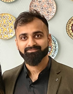 Prof. Awanish
Pandey
Prof. Awanish
Pandey
PROGRAMME COORDINATOR
Assistant Professor
OPTICS AND PHOTONICS CENTRE, INDIAN INSTITUTE OF TECHNOLOGY DELHI, NEW DELHI.
Prof. Awanish
Pandey is an Assistant Professor at the Optics and Photonics Centre, IIT Delhi. He has nearly a decade
of experience in semiconductors technology, having worked with leading semiconductor foundries like
imec, Belgium, and renowned research facilities such as CERN in Geneva, Switzerland. He obtained his
Ph.D. from the Indian Institute of Science, Bangalore in 2019. Primarily, his research works revolves
around manipulating the flow of photons in nanophotonic structures made of semiconductors such as
Silicon. Currently, his research group is focusing on developing ultra-high-speed integrated photonic
links and systems for 6G communication. Additionally, he plays a key role in the National Quantum
Mission (NQM), contributing to the development of India’s first photonic quantum processor.
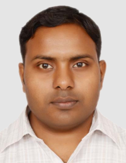 Prof.
Dheeraj
Prof.
Dheeraj
Assistant Professor
OPTICS AND PHOTONICS CENTRE (OPC), INDIAN INSTITUTE OF TECHNOLOGY DELHI, NEW DELHI.
Dheeraj
Pratap is an Assistant Professor at the Optics and Photonics Centre (OPC) of the Indian Institute of
Technology (IIT) Delhi. He obtained his PhD degree in metamaterials from the IIT Kanpur in 2016.
Later, he was a postdoctoral researcher in GRESPI at the University of Reims Champagne-Ardenne,
France. For a short time, he worked as a project scientist at the IIT Kanpur and then as an Assistant
Professor at the Veermata Jijabai Technological Institute (VJTI) Mumbai. Before joining the OPC, he
was a CSIR-Nehru Science Postdoctoral Fellow at the CSIR-Central Scientific Instruments Organization
(CSIO) in Chandigarh. His research interests include photonic metamaterials, metasurfaces, plasmonics,
and photothermal effects. He has published several research articles in national and international
journals of repute and has a few patents.
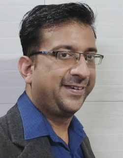 Prof. Deepak
Jain
Prof. Deepak
Jain
Assistant Professor
OPTICS AND PHOTONICS CENTRE (OPC), INDIAN INSTITUTE OF TECHNOLOGY DELHI, NEW DELHI.
Deepak
Jain is an Assistant Professor at the Optics & Photonics Center (OPC) of the Indian Institute of
Technology Delhi. Before this, he was an Assistant Professor at the Electrical Engineering department
of the Indian Institute of Technology Bombay, a University Research Fellow at the University of
Sydney, and a Hans Christian Oersted and Marie-Curie Research Fellow at the Technical University of
Denmark. He obtained his Ph.D. from the Optoelectronics Research Center, University of Southampton,
UK, and his MTech from the Indian Institute of Technology Kanpur. His area of interest revolves around
semiconductor, optical fibers, and technology transformation from academia to industry. He is a
co-founder of DeepLase Technologies and BrahmaSens Technologies, Delhi-based laser and sensor company
respectively, SpecPhotonics, an Adelaide-based specialty optical fiber company, and was an early
co-founder of NORBLIS, a Danish broadband laser company. He has more than 70 publications, including
30 journal publications and several invited conference papers. He is also a senior member of Optica
and IEEE