
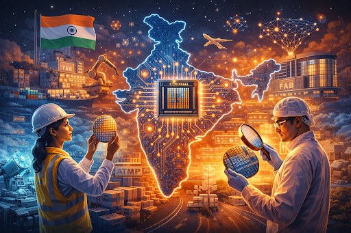
India’s semiconductor ambition has moved from aspiration to structured execution. With global chip supply chains undergoing fundamental realignment, India is positioning itself as a high-value contributor across design, fabrication, testing, and advanced packaging. The convergence of manufacturing capability, policy momentum, and talent development is enabling India to build a long-term foothold in a sector previously dominated by a handful of global players.
Written through the lens of a Senior Expert in semiconductor engineering and an IIT alumna known for her work in AI-enabled manufacturing systems, this analysis explores the core technological, strategic, and workforce elements shaping India’s semiconductor ecosystem. Her insights draw from years of experience conducting executive sessions, industry seminars, and academic workshops on transforming chip fabrication with artificial intelligence.
Table of Contents
- Strategic Policy Foundations: Building the National Semiconductor Mission
- Technology Maturity: AI-Driven Fabrication & Process Innovation
- Supply Chain Transformation: Localisation, ATMP Expansion & Global Alignment
- Manufacturing Scale-Up: ATMP to FAB – The Road to High-Volume Production
- Talent Pipeline: Engineering Skills Driving India’s Semiconductor Future
- Key Takeaways
- FAQs
Strategic Policy Foundations: Building the National Semiconductor Mission
India’s semiconductor roadmap is underpinned by strong policy frameworks designed to
attract global investment, build domestic capabilities, and strengthen supply
resilience. The Production-Linked Incentive (PLI) scheme, the Design-Linked Incentive
(DLI) program, and the India Semiconductor Mission (ISM) collectively aim to develop a
mature ecosystem spanning silicon fabrication, ATMP (Assembly, Testing, Marking &
Packaging), and compound semiconductor manufacturing.
Key priorities include:
- High-quality fabrication facilities (FABs)
- Localisation of ATMP and OSAT units
- Incentives for design startups and IP development
- AI-enabled automation for yield optimisation
- Partnerships with global technology leaders
These initiatives provide industry-wide direction and long-term stability for investors
and manufacturers.
Professionals who aim to contribute to policy-aligned manufacturing initiatives
increasingly pursue an advanced
semiconductor manufacturing program to understand how global supply chains,
process technologies, and government incentives intersect.
Technology Maturity: AI-Driven Fabrication & Process Innovation
The future of semiconductor manufacturing is defined by precision, automation, and
AI-driven process intelligence. India's ecosystem is rapidly embracing AI-enabled wafer
inspection, defect classification, predictive maintenance, process control, and material
flow optimisation.
Key areas of technological acceleration include:
- EUV and DUV lithography readiness
- Advanced deposition and etching methods
- Yield-enhancing algorithms using deep learning
- Inline metrology powered by image analytics
- Automated fault detection in nanometer-scale processes
India’s engineering clusters are building capabilities not just in traditional
semiconductor processes but also in emerging fields such as compound semiconductors and
photonics.
Engineers transitioning into these specialised domains often pursue a professional
course in semiconductor technology to gain a structured understanding of process
flows, AI-enabled inspection, and next-generation fabrication technologies.
Supply Chain Transformation: Localisation, ATMP Expansion & Global Alignment
India’s semiconductor strategy recognises that fabrication cannot exist in isolation. The
country is simultaneously strengthening upstream and downstream supply chains—from
speciality gases and wafers to ATMP and OSAT facilities. Partnerships with global firms
have accelerated investment in testing, packaging, and memory assembly plants, allowing
India to build foundational capacity ahead of full-scale wafer FAB operations.
Rapid developments include:
- ATMP plants by global majors entering Gujarat and Telangana
- Collaborations for substrate, packaging, and bonded wafer production
- Localisation of speciality chemicals and cleanroom manufacturing components
- Strengthening logistics and controlled-environment infrastructure
- AI-driven inventory and supply chain optimisation
These advancements help India plug into global networks that demand reliability,
precision, and large-scale throughput.
Supply chain and operations engineers expanding into high-tech manufacturing frequently
opt for a Semiconductor
course for working professionals to build competence in ATMP workflows,
materials handling, and supply chain synchronisation within fabrication pipelines.
Manufacturing Scale-Up: ATMP to FAB – The Road to High-Volume Production
India’s semiconductor growth strategy is evolving in stages. ATMP facilities form the foundation, but the long-term objective is full-scale FAB operations capable of producing mature and advanced nodes. This transition requires alignment of:
- Equipment sourcing and installation expertise
- Cleanroom engineering and contamination control
- Process automation and digital twins
- Material purity and quality assurance frameworks
- AI-driven predictive process control
India’s early-stage focus on mature nodes (28 nm, 65 nm) is a strategic stepping stone.
These nodes have high commercial demand in automotive electronics, IoT, telecom
equipment, and industrial automation.
Mid- to senior-level managers overseeing scale-up efforts often pursue a semiconductor
executive certification to gain strategic insight into global manufacturing
benchmarks, operational KPIs, and long-term industry transitions from ATMP to
high-volume wafer FABs.
Talent Pipeline: Engineering Skills Driving India’s Semiconductor Future
The semiconductor industry requires an advanced talent pipeline spanning materials
science, process engineering, automation, device physics, lithography, and AI-driven
defect analytics. With India’s manufacturing and design ecosystem expanding rapidly, the
demand for skilled professionals is entering a high-growth phase.
Key skill clusters seeing demand include:
- VLSI design and verification
- Lithography, etching, deposition and CMP process engineering
- Semiconductor materials and device characterisation
- Packaging engineering and reliability testing
- AI-enabled process control and wafer inspection
- Cleanroom operations and contamination prevention
The author, in her role as an industry mentor and technical speaker, highlights the
importance of cross-disciplinary training that merges semiconductor physics with machine
intelligence and high-precision manufacturing systems.
Engineers entering this talent pipeline often explore a Semiconductor
Manufacturing Programme India to align their learning with industry requirements
in process technology, automation, and fabrication workflow design.
Key Takeaways
- India is building a coordinated semiconductor ecosystem driven by policy, technology, and workforce development.
- AI-enabled manufacturing will define the next wave of innovation and yield optimisation.
- Localisation of supply chains—from wafer production to ATMP—is accelerating manufacturing readiness.
- Strategic investments in mature nodes and packaging form the stepping stones to advanced FABs.
- Talent development across VLSI, process engineering, materials science, and AI-driven automation is essential for long-term growth.
- Structured semiconductor education and executive programs are supporting India’s emerging workforce needs.