
Every technology cycle produces a moment when the cost of not upskilling begins to exceed the cost of doing so. Engineers and technology leaders who lived through the transition from analogue to digital, or from desktop software to the internet, will recognise the pattern. The professional who had the technical foundation to move with the shift found that their career options expanded dramatically. Those who did not find the opposite, that their existing expertise, however deep, was being treated as less relevant with each passing year.
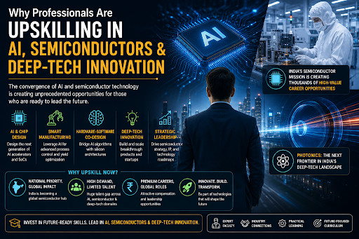
The convergence of artificial intelligence and semiconductor hardware is that moment, replayed at a scale and speed that is arguably unprecedented. The chips that power AI systems are no longer commodity products sourced from a handful of established suppliers. They are the central object of geopolitical competition, industrial policy, and the most capital-intensive wave of infrastructure investment the technology industry has seen. India is positioning itself as a significant participant in that wave, and the professionals who understand how AI workloads are translated into silicon, and how silicon is designed, manufactured, and deployed, are being sought with an urgency that is rewriting compensation structures and career trajectories in real time.
This is the context in which India's most forward-looking engineering professionals are making a deliberate choice to invest in structured upskilling. It is not a response to job insecurity. It is a recognition that an extraordinary window of professional opportunity is open and that it will not remain so indefinitely for those who observe it without acting.
Table of Contents
- India's Semiconductor Ambitions Are Generating Real Demand
- Who is Upskilling & What They Are Trying to Solve
- The Entrepreneurial Imperative in Deep-Tech Hardware
- What a Well-Designed Executive Programme Delivers & What It Cannot Replace
- The AI-Semiconductor Relationship: Understanding Both Directions
- Photonics as the Next Frontier in India's Deep-Tech Landscape
- The Timing Argument: Why Now Specifically
- A Field That Rewards the Prepared
- FAQs
India's Semiconductor Ambitions Are Generating Real Demand
The policy architecture supporting India's semiconductor ambitions is now substantial enough that it is no longer primarily a statement of intent; it is a driver of actual hiring. The India Semiconductor Mission, with its multi-billion-dollar incentive framework, has attracted commitments from Tata Electronics, Micron Technology, and a cluster of ATMP and OSAT investors that are collectively creating thousands of engineering roles that did not exist three years ago. The Tata-PSMC fabrication facility in Gujarat, when operational, will represent a different category of industrial asset for India, one that requires process engineers, equipment specialists, yield analysts, and quality systems professionals trained to the standards of advanced semiconductor manufacturing.
Alongside the fab-level investment, the fabless chip design ecosystem is expanding. Established semiconductor multinationals are deepening their India design centres, and a new generation of domestic fabless startups, several backed by serious venture capital, are building original silicon for AI inference, automotive systems, and defence electronics. The talent they need has a specific profile: engineers who understand chip design at depth, who are fluent in the architectures that AI workloads demand, and who can collaborate across the hardware-software boundary that modern AI systems require. That profile is not easy to find, and the gap between demand and supply is the primary driver of the upskilling momentum the industry is currently experiencing.
Who is Upskilling & What They Are Trying to Solve
The professionals making this investment are not homogeneous. They include chip design engineers who have spent years working in VLSI but now see the entire value proposition of their domain being reorganised around AI-specific architectures. They include software engineers and AI researchers who have built sophisticated machine learning systems but recognise that the hardware constraints of real-world deployment require an understanding of the silicon that their models run on. They include manufacturing and process engineers in electronics companies who are watching AI-driven quality systems and fab automation tools reshape their discipline. And they include technology managers and R&D leaders who need the strategic vocabulary to make decisions about semiconductor investments, IP development, and deep-tech venture creation.
The table below maps specific professional backgrounds to the upskilling needs those backgrounds generate and to the career outcomes that structured, advanced training in this domain makes possible:
| Professional Background | Immediate Upskilling Need | Strategic Career Outcome |
|---|---|---|
| VLSI / Chip Design Engineer | AI hardware architecture, neural accelerator design | Lead AI chip programmes; move into architecture or product roles |
| Electronics & Embedded Systems Engineer | Edge AI, FPGA-based inference, sensor-to-cloud integration | Senior systems architect in smart manufacturing or automotive AI |
| Software / AI Research Engineer | Semiconductor physics, hardware-software co-design, RTL fundamentals | Bridge role between AI teams and silicon design divisions |
| Manufacturing / Process Engineer | AI-driven yield optimisation, defect detection, and statistical process control | Process integration lead or AI-enabled fab operations head |
| R&D Scientist (Physics / Materials) | Photonic device integration, compound semiconductors, device modelling | Senior researcher or CTO in photonics or deep-tech hardware startup |
| Technology Manager / Engineering Leader | Semiconductor ecosystem strategy, IP management, deep-tech venture dynamics | VP Engineering, CTO, or founding team member of hardware ventures |
| Defence / Aerospace Engineer | Custom silicon for secure communications, radiation-hardened design, ITAR-compliant sourcing | Lead indigenous semiconductor programmes for defence modernisation |
The pattern across all of these profiles is the same: an existing foundation of technical expertise that is genuinely valuable, combined with a gap at the AI-semiconductor interface that structured education is the most efficient way to close. Self-study can address parts of this gap. There is no shortage of online resources in semiconductor engineering and AI hardware. But the depth, the integration across disciplines, the peer learning with other experienced professionals, and the institutional credibility that a well-designed executive programme provides are not replicable through informal pathways alone.
The Entrepreneurial Imperative in Deep-Tech Hardware
One dimension of the upskilling conversation that deserves particular attention is the growing number of senior professionals who are not simply looking to advance within existing organisations but who are considering the founding of deep-tech hardware ventures. India's startup ecosystem has matured considerably, and the capital available for serious semiconductor and AI hardware companies from dedicated deep-tech funds, from strategic corporate investors, and from government programmes like iDEX and the Startup India semiconductor track is at levels that make hardware entrepreneurship a genuinely viable path for technically credentialled founders. A structured Deep-Tech Entrepreneurship Programme India, specifically oriented towards semiconductor and AI professionals, addresses a gap that has historically limited the conversion of technical expertise into commercial ventures: the business, legal, financial, and strategic knowledge that technical founders need to build organisations, not just products.
Building a hardware company is different from building a software startup in ways that extend well beyond the obvious differences in capital requirements and development timelines. An IP strategy for semiconductor innovations is complex and consequential. The difference between owning a defensible patent portfolio and building on technology that cannot be protected can determine whether a company is fundable and whether it survives competitive pressure from larger players. Supply chain strategy for a fabless company requires understanding of foundry relationships, packaging and test ecosystems, and lead time dynamics that have no real analogue in software. Regulatory compliance for defence-adjacent electronics, medical devices, and telecommunications equipment adds further layers of complexity. The professionals who emerge from a rigorous entrepreneurship programme with these competencies, layered on top of deep technical expertise, represent the most capable founding profiles in the deep-tech hardware space.
What a Well-Designed Executive Programme Delivers & What It Cannot Replace
The Executive Programme in Semiconductors, AI, and Deep-Tech Entrepreneurship is built around a specific conviction: that the professionals who will lead India's semiconductor decade are not blank slates who need foundational education, but experienced engineers and technology leaders who need an integrated, advanced, and institutionally credible framework for the intersection of domains that they are already operating in. An AI and Semiconductor Executive Course of this calibre does not begin with introductory electronics. It begins with the assumption that its participants understand engineering, and moves directly into the questions that the industry's most important current challenges are asking: How are neural processing units architected to maximise throughput per watt? How are AI-based defect detection systems integrated into semiconductor process monitoring workflows? How do you evaluate a chip startup's IP portfolio for investment or acquisition? These are not classroom hypotheticals. They are live questions in the organisations that participants work in and lead.
The peer learning dimension of a well-curated executive cohort is one of its most underestimated assets. When a process engineer from a major electronics manufacturer sits alongside a chip design architect from a fabless startup and a former academic who has recently moved into a corporate R&D role, the conversations that happen outside formal sessions about deployment realities, design trade-offs, organisational dynamics, and market intelligence constitute a form of learning that no curriculum can fully replicate. Executive programmes that attract a genuinely diverse and experienced cohort are providing access to a professional network that compounds in value over an entire career.
The AI-Semiconductor Relationship: Understanding Both Directions
A recurring misconception in conversations about AI and chip engineering is that the relationship runs in one direction, that AI is the application, and semiconductors are the infrastructure that supports it. The reality is bidirectional, and understanding both directions is essential for professionals who want to operate at the frontier of the field. Semiconductor Technology for AI means understanding not only the custom chip architectures, the tensor processing units, the neural processing units, the in-memory computing designs that AI workloads demand, but also the ways in which AI techniques are transforming semiconductor manufacturing itself. Predictive maintenance algorithms that anticipate equipment failure in lithography tools. Computer vision models trained on wafer inspection data to detect defect patterns that human operators miss. Reinforcement learning systems that optimise process recipes for yield improvement across thousands of variables simultaneously. These applications of AI within fabs are not speculative. They are deployed at leading-edge manufacturing facilities globally, and as India's own fabrication infrastructure scales, the professionals who can implement and operate these systems will be among the most sought-after in the industry.
This bidirectional framing AI for chips, and chips for AI, is one of the conceptual anchors of serious advanced programmes in this space. It ensures that graduates are not trained to operate in one direction of the relationship while remaining naive about the other, which is the limitation of programmes that address either AI or semiconductor engineering in isolation.
Photonics as the Next Frontier in India's Deep-Tech Landscape
Among the specialisations gaining momentum within India's semiconductor talent development agenda, photonics occupies a strategically significant position. Silicon photonics, the integration of optical components into semiconductor platforms to enable data transmission using light, is moving from research laboratories into commercial production at a pace that is accelerating demand for engineers who can work at the photonic-electronic interface. Optical interconnects for data centres, LiDAR systems for autonomous vehicles, photonic chips for quantum computing applications, and defence optoelectronics systems under the Atmanirbhar Bharat programme are all driving this demand. A Semiconductor and Photonics course that integrates classical semiconductor process knowledge with the principles of optical device design, waveguide engineering, and optoelectronic integration addresses a specialisation that is currently underpopulated relative to the opportunities it is being asked to fill.
India has a strong academic foundation in photonics; several IITs and IISc have groups with internationally recognised research output in this domain. The current challenge is translating that research capability into the industrial engineering competencies that commercial photonics manufacturing requires. Executive programmes that include structured photonics content are providing a bridge for professionals with adjacent expertise, those from communications, defence electronics, or semiconductor process engineering, to develop the specific competencies that this frontier demands. Given the growth trajectory of the photonics market globally and the specific domestic demand drivers in India, this is a specialisation that warrants serious strategic attention from professionals planning their next decade.
The Timing Argument: Why Now Specifically
The argument for upskilling in AI and semiconductors is not new. The argument for doing it now, specifically, rests on a set of conditions that are unlikely to persist indefinitely. The first is that India's semiconductor infrastructure is not yet fully built. The professionals who develop advanced competencies in this domain during the construction phase of India's semiconductor industry will occupy foundational positions in it. They will be the senior engineers, the technical directors, the programme leads, and in many cases the founders of the organisations that define what India's chip ecosystem looks like a decade from now. That kind of career positioning is only available during a window of industrial formation, not after the field has matured and its senior ranks are already filled.
The second is that the executive programmes available today are being developed with the direct involvement of an industry that is actively shaping their content. Faculty with genuine industry exposure, curriculum committees that include practitioners from leading semiconductor companies, and capstone projects that engage with real industrial problems are features of programmes designed during a period when the industry is eager to help build the talent pipeline it needs. These conditions produce programmes of a quality and relevance that is harder to sustain once the urgency diminishes.
A Field That Rewards the Prepared
Semiconductor engineering has always been a discipline that rewards depth. The physics are demanding, the processes are unforgiving, and the system-level complexity of integrating billions of transistors into a functional device requires a kind of rigorous, multi-scale thinking that does not develop casually. Artificial intelligence, at the hardware level, adds another layer of complexity, one that requires understanding machine learning workloads not just as software abstractions but as computational patterns with specific implications for memory hierarchy, power delivery, data movement, and numerical precision.
The professionals who are choosing to develop this integrated capability, who are investing in executive programmes that take both their experience and the frontier of the field seriously, are making a bet that the evidence strongly supports. The industry needs them. The infrastructure to deploy them is being built. The institutional and policy support for their professional development is in place. And the career trajectories of those who move early, with the right preparation, in a field undergoing the kind of structural expansion that India's semiconductor ecosystem is currently experiencing, have historically been exceptional.
The window is open. The question is what each professional does with the time it offers.